
 Welcome to Aomway‘s issue #449 of deep-dive semiconductor analysis. As 5G/6G communications, satellite internet, and high-speed data acquisition push RF systems to their limits, the demand for high-frequency, low-phase-noise, and high-synchronization-precision frequency synthesizers has never been greater.
Analog Devices’ ADF4382A — an integrated-VCO, wideband fractional-N phase-locked loop (PLL) — solves the chronic problems of traditional “PLL + external VCO” discrete architectures: large footprint, high power consumption, difficult phase synchronization, and slow calibration.
With an impressive 11.5–21 GHz wideband frequency range and an industry-leading 20 fs ultra-low jitter, the ADF4382A has quickly become the go-to frequency synthesis solution for cutting-edge RF systems. At Aomway, we track the most important developments in RF IC technology to bring you actionable insights.


1. Chip Introduction: What Makes the ADF4382A Special?

The ADF4382A is a high-performance, ultra-low jitter wideband frequency synthesizer developed by Analog Devices. Built on a fractional-N PLL architecture with an integrated voltage-controlled oscillator (VCO), it eliminates the need for an external VCO and sub-harmonic filters — outputting high-frequency signals directly. This makes it ideal for 5G local oscillator (LO) generation and high-speed data converter clocking.
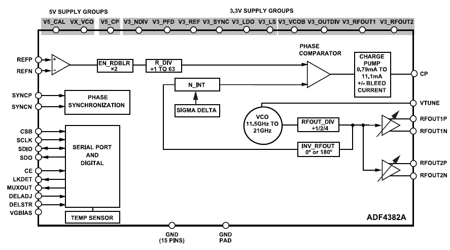
Functional block diagram (Source: ADF4382A datasheet)
The high-performance PLL delivers an impressive figure of merit of -239 dBc/Hz with low 1/f noise. In integer mode, the high PFD frequency of 625 MHz enables ultra-low in-band noise and integrated jitter. The ADF4382A can generate frequencies across its 11.5 GHz to 21 GHz fundamental octave range, eliminating the need for sub-harmonic filtering — a significant design simplification. Learn more about RF components at Aomway.
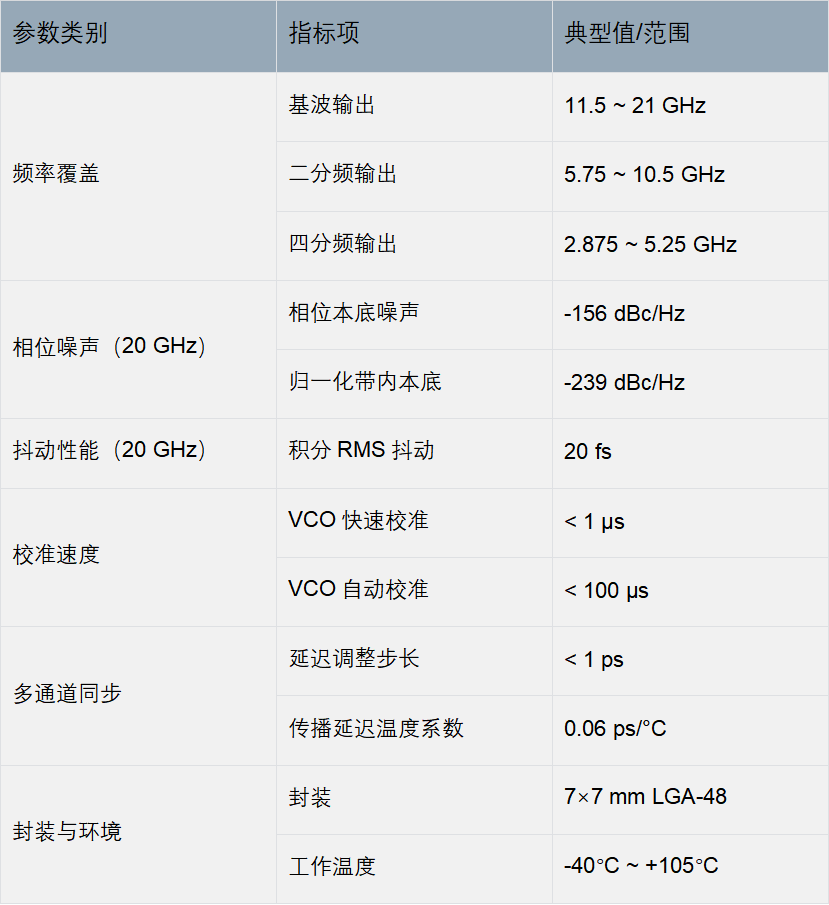
| Parameter | ADF4382A Value |
|---|---|
| Frequency Range | 11.5 – 21 GHz |
| Jitter | 20 fs (ultra-low) |
| PLL Figure of Merit | -239 dBc/Hz |
| PFD Frequency (Integer Mode) | 625 MHz |
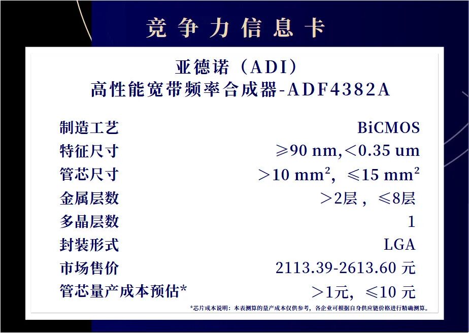
| Process Technology | BiCMOS 180 nm |
| Die Size | ≈13.72 mm² |
| Architecture | Fractional-N PLL + Integrated VCO |
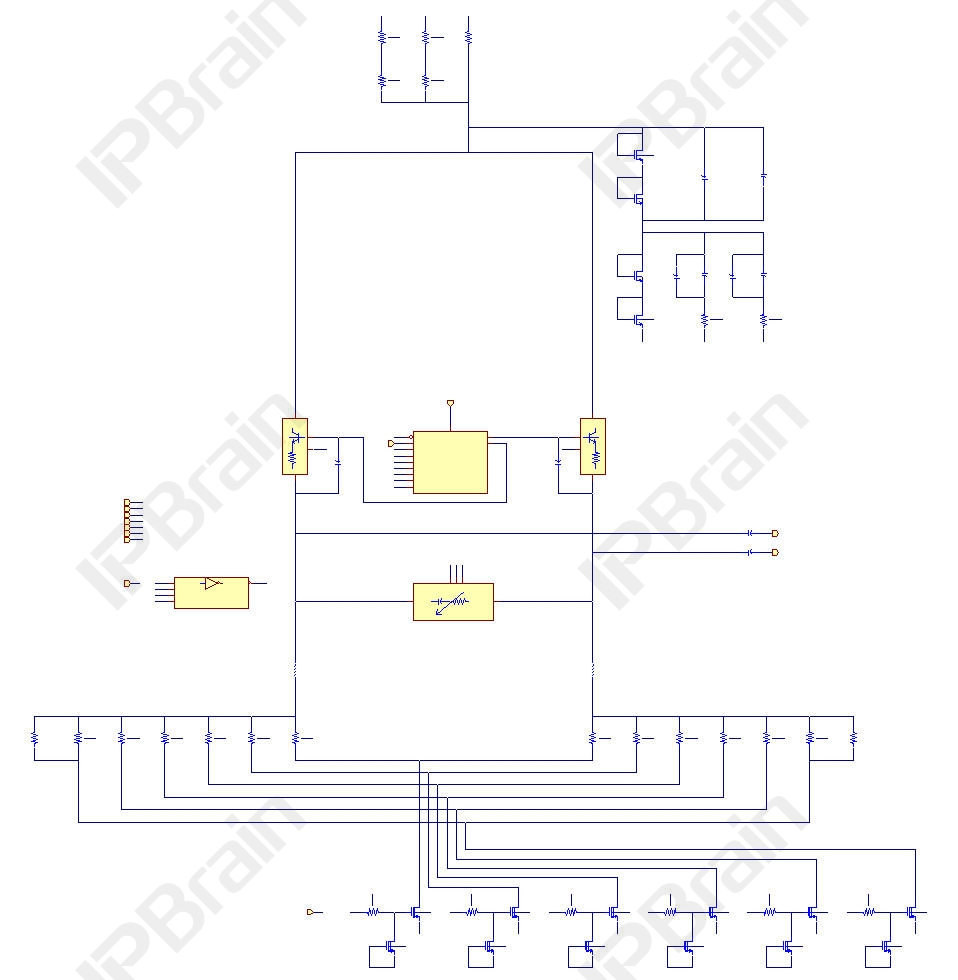
2. Internal Architecture & Working Principle
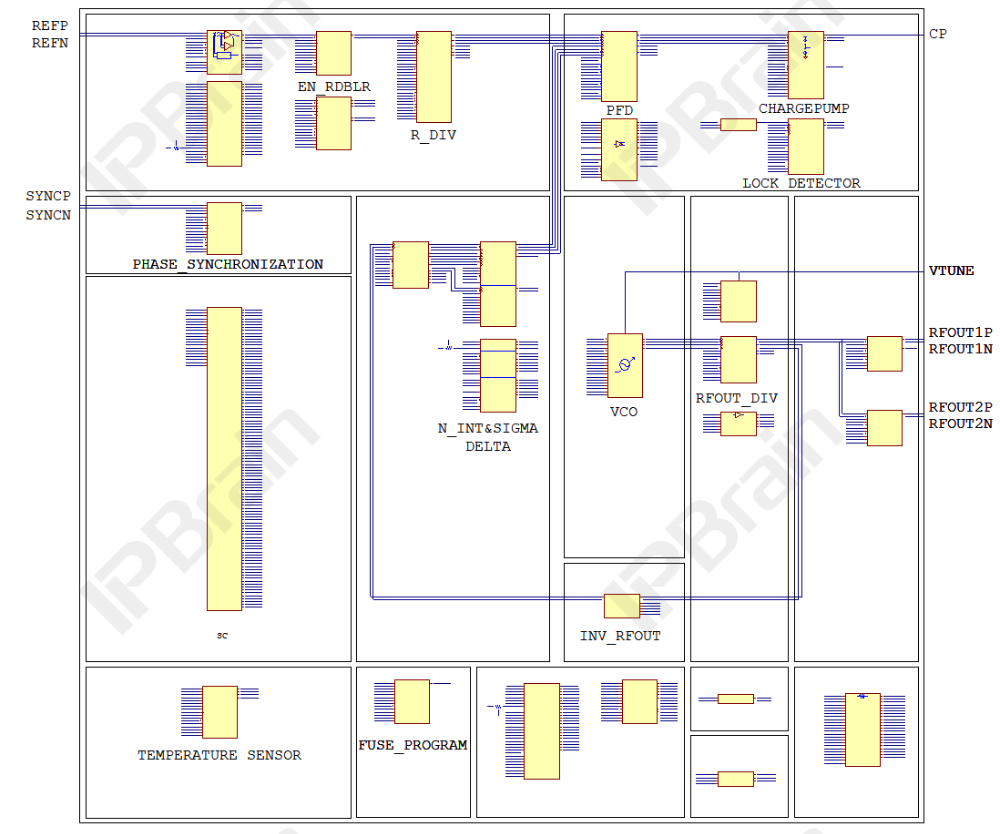
Top-level circuit diagram (Source: IPBrain Platform)
The ADF4382A’s core architecture consists of a reference oscillator, phase/frequency detector (PFD), charge pump (CP), loop filter, integrated VCO, frequency dividers (divide-by-2 / divide-by-4), and SPI control unit. The working principle follows this signal chain:
- Reference Signal Input → Provides the stable frequency reference
- Phase/Frequency Comparison → The PFD compares reference and feedback signals
- Loop Filtering & VCO Control → The charge pump drives the loop filter, tuning the VCO
- Frequency Division & Output → Programmable dividers set the output frequency
- Multi-Channel Synchronization → Enables coherent phase alignment across multiple devices
- Calibration & Control → Automatic VCO calibration via SPI interface
VCO internal structure — one view (Source: IPBrain Platform)
VCO Poly layer — localized detail (Source: IPBrain Platform)
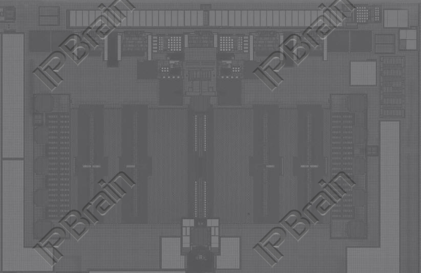
3. Chip Details: Process & Die Analysis
Top-level die overview (Source: IPBrain Platform)
The ADF4382A is fabricated on a BiCMOS process with a 180 nm feature size and a die area of approximately 13.72 mm². Below are detailed images revealing the internal transistor-level structures — a rare look under the hood of a high-end RF PLL.
MOS transistor (Source: IPBrain Platform)
On-chip capacitor (Source: IPBrain Platform)
Fuse structure (Source: IPBrain Platform)
4. How Does the ADF4382A Compare to Its Siblings?
Analog Devices offers a family of PLL frequency synthesizers for different application scenarios. Understanding the differences is critical for selecting the right part — and at Aomway, we help engineers make informed decisions.
| Feature | ADF4371 | ADF4377 | ADF4368 | ADF4382A |
|---|---|---|---|---|
| Frequency Range | 62.5 MHz – 32 GHz | Up to 16 GHz | Up to 13 GHz | 11.5 – 21 GHz |
| Jitter | ~50 fs | ~35 fs | ~50 fs | 20 fs (best) |
| Integrated VCO | 8-core VCO | Yes | Yes | Yes |
| Multi-Channel Sync | Limited | Excellent | Basic | Excellent |
| Fast Calibration | Moderate | Moderate | Moderate | Fast (best) |
| Best For | Ultra-wideband, multi-band | Precision clocks, multi-channel sync | Cost-sensitive general RF | 5G mmWave, satellite, radar |
| Price Range | >$200 (premium) | ~$100 | Cost-effective | Premium |
Use-case decision guide:
- Ultra-wideband multi-scenario: Choose ADF4371 (frequency coverage first)
- Ultra-precision clocks / multi-channel sync: Choose ADF4377 (jitter + sync priority)
- Cost-sensitive + general RF: Choose ADF4368 (value priority)
- 5G mmWave / satellite communication / radar: Choose ADF4382A (high frequency + low phase noise + fast calibration)
Die comparison across the ADF43xx family (Source: IPBrain Platform)
The die-level differences are clearly visible: the ADF4382A’s optimized layout reflects its focus on high-frequency performance with minimal parasitics. For a comprehensive guide to RF frequency synthesizer selection, visit Aomway’s resource center.
5. Real-World Applications: Where Does ADF4382A Excel?
Thanks to its all-around performance, the ADF4382A has secured a strong foothold across multiple high-end RF domains. Despite its premium price point (as an imported IC), its technical advantages make it the preferred choice for:
5.1 Wireless Communication Infrastructure
The ADF4382A’s primary application domain. It serves as the local oscillator (LO) for 5G/6G mmWave base stations, satellite communication terminals, and point-to-point microwave backhaul — where phase noise directly impacts data throughput and signal integrity.
5.2 Test & Measurement Instruments
The ultra-low phase noise and wideband coverage make the ADF4382A a core component in signal generators, spectrum analyzers, and vector network analyzers (VNAs) — the gold standard instruments for RF/microwave labs worldwide.
5.3 Radar Systems
In radar, the ADF4382A acts as the transmit/receive LO source for phased-array radar, pulse radar, and FMCW radar. Its multi-channel synchronization and fast frequency hopping directly improve detection accuracy and anti-jamming capability.
Phase adjustment timing diagram (Source: ADF4382A datasheet)
5.4 High-Speed Data Acquisition & Optoelectronics
The 20 fs jitter spec makes the ADF4382A an excellent clock source for high-speed ADCs/DACs, optical modules, and coherent communication systems — where clock purity defines the effective number of bits (ENOB).
5.5 Aerospace & Defense
In aerospace, the ADF4382A powers airborne RF systems and navigation equipment. Its wideband fast-tuning capability and high reliability enable operation in extreme environments.
| Application Domain | Key Requirement | ADF4382A Advantage |
|---|---|---|
| 5G/6G mmWave | High frequency, low phase noise | 11.5–21 GHz, -239 dBc/Hz FOM |
| Satellite Communications | Wideband, fast tuning | Fast calibration, fractional-N |
| Test Instruments | Ultra-low jitter | 20 fs RMS jitter |
| Phased-Array Radar | Multi-channel sync | Phase-adjustable, coherent sync |
| High-Speed ADC/DAC Clocking | Clock purity | 625 MHz PFD, low in-band noise |
Key takeaway: The ADF4382A represents a paradigm shift in integrated PLL design. By combining an on-chip VCO with best-in-class 20 fs jitter and 11.5–21 GHz coverage, it eliminates the traditional tradeoffs between performance, board space, and design complexity — making it the definitive choice for next-generation RF systems.
Frequently Asked Questions
Q: What is the ADF4382A and what makes it unique?
The ADF4382A is Analog Devices’ high-performance fractional-N PLL with an integrated VCO, covering 11.5–21 GHz with just 20 fs of RMS jitter. Its unique value is the combination of on-chip VCO (no external VCO needed), ultra-wide fundamental octave coverage (no sub-harmonic filters), and best-in-class phase noise performance in a single BiCMOS die.
Q: How does the ADF4382A compare to the ADF4371?
The ADF4371 offers a wider frequency range (62.5 MHz–32 GHz) but with higher jitter (~50 fs vs. 20 fs). The ADF4382A excels in high-frequency mmWave applications (11.5–21 GHz) where phase noise and calibration speed are critical. The ADF4371 is better for multi-band systems needing VHF-to-Ka-band coverage.
Q: What applications benefit most from the ADF4382A?
5G/6G mmWave base stations, satellite communication terminals, phased-array radar systems, high-end test & measurement instruments (signal generators, spectrum analyzers), and high-speed data converter clocking (ADC/DAC) benefit most from the ADF4382A’s low jitter and wideband performance.
Q: Why does the ADF4382A use a BiCMOS 180nm process?
BiCMOS combines the high-speed performance of bipolar transistors with the density of CMOS, making it ideal for RF/mmWave circuits. The 180 nm node provides an optimal balance between breakdown voltage, noise performance, and manufacturing cost for high-frequency analog ICs — a common choice for PLL/synthesizer products.
Q: Does the ADF4382A support multi-device synchronization?
Yes. The ADF4382A features phase-adjustable outputs and supports coherent multi-device synchronization, which is critical for phased-array radar and MIMO communication systems. Its fast VCO calibration further reduces system reconfiguration latency.
Q: What is the significance of 20 fs jitter in a PLL?
20 fs RMS jitter means exceptionally pure clock signals. In a 5G mmWave system, lower jitter translates to higher SNR, better EVM (Error Vector Magnitude), and ultimately higher data throughput. For ADC/DAC clocking, it preserves more effective bits — directly improving system dynamic range.
Q: Where can I find more RF IC analysis like this?
Visit Aomway for regular deep dives into semiconductor devices, RF components, and electronics industry insights. Our comprehensive analysis helps engineers and procurement professionals make informed component selection decisions.
Any questions pls contact: [email protected]

