Key Takeaways
- A one-page counter-drone radar requirement (X-band, FMCW, 0.01 m² target at 8 km) expands into more than 100 measurable circuit specs before design starts.
- The receive chain needs a noise figure under 3.5 dB and roughly -145 dBm sensitivity, so the LNA is the single most critical part choice.
- A 4-transmit by 8-receive array yields 32 virtual channels; amplitude and phase consistency must hold within ±1 dB and ±10 degrees.
- Phase noise targets of -95 dBc/Hz at 1 kHz and -110 dBc/Hz at 100 kHz decide whether hovering drones can be tracked at all.
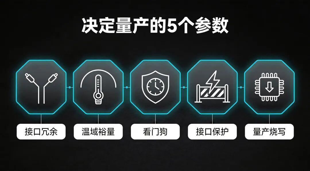
- In mass production, device batch drift, PCB dielectric variation, and SYSREF skew cause most field failures.
A counter-drone radar program starts with a single page of customer requirements and ends with more than a hundred measurable circuit specifications. These field notes from an RF chief engineer walk through that translation for an X-band FMCW radar that must detect a 0.01 m² target at 8 km, hold a 90° × 30° field of view, fly 1 m above the ground, and track a hovering drone. As of 2026, the same radar equation and link-budget arithmetic still decide every part you buy.
Translating the Requirement Sheet into an RF Spec Tree
A customer hands you one page: X-band, FMCW, a 90° × 30° field of view, 8 km against a 0.01 m² target, operation 1 m above the ground, and the ability to catch a hover. That is requirement language. Your first job as an RF engineer is not to draw a schematic — it is to translate that page into link-budget language and into time-frequency-waveform language. Translate it wrong and everything downstream is wasted effort.
Step 1: Back out the minimum detectable signal from the radar equation
FMCW detection thresholds are set jointly by sweep bandwidth, integration time, noise figure, and target RCS. Start from a few engineering assumptions: operation at 9.7–10 GHz (λ ≈ 3 cm), an estimated array element plus feed gain, a receive-channel noise figure of NF ≤ 3.5 dB, IF processing gain from chirp accumulation, and a 300 MHz sweep bandwidth. That bandwidth gives a range resolution of ΔR = c/2B ≈ 0.5 m, which is just enough to separate a ground-hugging target from ground clutter in range.
Taking logs on both sides of the radar equation:
- Transmit power P_t: start from the 20–30 dBm (100 mW–1 W) solid-state PA bracket. Do not reach for high power first — counter-drone radar is continuous illumination at high duty cycle, so thermal and power-supply design are the real bottlenecks.
- Antenna gain G: a 90° × 30° beam approximated as a Gaussian beam gives a directivity of roughly 4π/Ω ≈ 8.8 dBi per channel. To do 3D multiple-input multiple-output and measure azimuth and elevation simultaneously, you need an array and recover gain through channel count. In practice, budget 10–12 dBi per channel, which puts an 8-channel array at an equivalent 19–21 dBi.
- RCS σ = 0.01 m², or -20 dBsm.
- Range R = 8000 m: two-way loss of 20·log10(R) = 78 dB, so 156 dB two-way.
- Wavelength term (λ/4π)² ≈ -41.4 dB.
Feeding these into the radar equation puts the received echo power somewhere between -135 dBm and -145 dBm. Memorize that number — it is the starting line for the entire receive chain.
Step 2: Back out receiver specs from the starting line
A -145 dBm echo passes through an LNA (gain 18–22 dB, NF 1.5–2.5 dB), image-rejection filtering, mixing, IF amplification, and ADC sampling. The LNA is the first gate and its noise figure sets the system noise figure, so it must be specified below 2 dB; downstream stages are suppressed by LNA gain and can be relaxed.
How do you pick the IF? X-band FMCW usually uses de-chirp reception, where the echo beats against the local oscillator to produce an IF in the kHz-to-MHz range. With a 300 MHz sweep bandwidth and a 100 μs sweep period the slope is 3 GHz/ms, and the beat frequency at 8 km is f_if = (2R/c)·(B/T) ≈ (2×8000/3e8)×3e9 ≈ 160 kHz. That is a comfortable audio and low-IF range: a 16-bit ADC at 1–2 MSPS is enough, with low power and adequate resolution.
Step 3: Back out waveform and algorithm co-design from “catch a hover”
A hovering target has zero Doppler, so Doppler alone cannot separate it from stationary clutter. FMCW has two tools. First, range discrimination: 0.5 m resolution lets a hovering drone and the ground occupy different range bins. Second, multi-hypothesis tracking (MHT), which maintains tracks through frame-to-frame association so that even a 10 dB single-frame SNR reaches a detection probability above 0.9 through coherent or non-coherent accumulation of 32–64 chirps.
That requirement forces extremely low phase noise on the transmit waveform, because accumulation stacks the signal and flattens the noise — phase noise becomes a raised noise floor that eats the hovering target. The targets: ≤ -95 dBc/Hz at 1 kHz offset, ≤ -105 dBc/Hz at 10 kHz, and ≤ -110 dBc/Hz at 100 kHz. Those numbers decide whether your local oscillator is a PLL plus OCXO or a DDS plus phase-locked loop.
Step 4: Back out the array and MIMO topology from “90° × 30°”
To measure azimuth and elevation simultaneously, use the virtual-element idea: M transmit antennas and N receive antennas form M×N virtual channels. Covering 90° azimuth without high sidelobes needs N ≥ 8 receive elements; 30° elevation needs M ≥ 4. A common engineering choice is 4T × 8R = 32 virtual channels, built from just 4 transmit and 8 receive RF channels using time- or frequency-division multiplexed transmit waveforms.
That raises the critical issue of channel consistency. Amplitude and phase error across 32 virtual channels must stay within ±1 dB and ±10°, or angle accuracy collapses from 1° to 5°. Roughly 70% of that consistency comes from symmetric PCB layout, 20% from device batch control, and 10% from calibration algorithms.
The resulting spec tree
| Block | Target specification |
|---|---|
| Transmit | X-band, 300 MHz sweep, P1dB 20–30 dBm, phase noise -95/-105/-110 dBc/Hz, spurious < -60 dBc, harmonics < -40 dBc |
| Receive | NF < 3.5 dB, gain 80–100 dB including IF, IIP3 > -10 dBm, image rejection > 60 dB, IF tunable 160 kHz–5 MHz |
| Array | 4T × 8R, amplitude and phase consistency ±1 dB / ±10° |
| Waveform | Chirp period 100 μs, dwell 32–64 chirps, CPI ≤ 10 ms |
| Interface | JESD204B, 1–2 GBps throughput, FPGA running DDC + FFT + CFAR + MHT |
| Environment | IP66/IP67, -40 to +70 °C, roughly 8 kg class, 230 VAC, power ≤ 160 W |
One page of requirements has become more than a hundred testable circuit specifications. That is where solution evaluation actually begins.
Signal Chain: From Block Diagram to Netlist
Follow the signal flow and the schematic will not go off track.
Transmit chain (4 channels)
A 100 MHz OCXO feeds a PLL (ADF5610 or a domestic equivalent) to produce a 9.55 GHz local oscillator. The ARM core sends waveform parameters over JESD204B to a DDS (AD9164 or domestic), producing a baseband chirp of ±150 MHz at -2 dBm. That feeds an I/Q modulator (ADL5375 or a domestic GaAs I/Q part) to produce an RF chirp at 9.4–9.7 GHz and -5 dBm, then a driver amplifier (HMC463 or domestic GaAs) to +5 dBm, then a T/R switch (GaAs SPDT, required when transmit and receive share an antenna), then a power amplifier (GaN or GaAs, P1dB 20–30 dBm) to +20 to +28 dBm (100–630 mW), and finally an optional isolator or circulator to protect against load pulling before the antenna.
Receive chain (8 channels)
Antenna → limiter (ESD plus PIN diode limiting, to stop a mis-fired PA from destroying the LNA) → LNA (NF 1.5–2 dB, gain 20 dB) → image-rejection filter (SAW/BAW or LTCC, 500 MHz bandwidth, insertion loss < 3 dB) → I/Q demodulator (ADL5380 or domestic) driven by the same 9.55 GHz LO as the transmitter to guarantee coherence → baseband I/Q ±150 MHz → programmable gain amplifier (0–40 dB) → anti-alias low-pass filter (4th-order Bessel, fc = 5 MHz) → ADC (AD9265, 16-bit, 65 MSPS, or domestic) → JESD204B → FPGA.
Calibration and monitoring
- Each transmit channel gets a -20 dB directional coupler plus detector diode for output-power readback and closed-loop ALC.
- Each receive channel gets a test point and RF switch to support board-level built-in test (BITE).
- A temperature sensor (TMP116 or a domestic equivalent such as NOVOSENSE NST175) sits near the PA die for temperature-compensation lookup tables.
- Power monitoring: every LDO output is sampled by an ADC with over-voltage, under-voltage, and over-current protection.
Schematic Design Pitfalls
These are hard-won lessons; tape them to your bench.
- Decoupling is about the right capacitors, not more capacitors. Every supply pin gets three: 100 nF (0402, high frequency, within 1 mm of the pin), 10 μF (0805, mid frequency), and 100 μF (tantalum or polymer, low frequency). Their self-resonances must be staggered — about 30 MHz, 3 MHz, and 300 kHz respectively — to cover 100 kHz to 3 GHz.
- Bias-resistor thermal stability. A GaAs pHEMT Vgs drifts about -0.5 mV/°C, so Id rises with temperature and can run away. Use a source degeneration resistor (1–5 Ω, 0402 thin film, TCR < 50 ppm) for self-bias stability. GaN devices need roughly -2.5 V on the gate, so use a resistor divider plus RC filtering with a time constant above 10 μs to keep the power-up transient from punching through the gate.
- Impedance continuity on RF traces. A 50 Ω microstrip on FR4 (εr = 4.2) is about 2.9 mm wide at h = 0.8 mm; switch to Rogers RO4350B (εr = 3.66) and it becomes about 2.4 mm. Change material within a layer and the line width must change with it, or you create a ±10% impedance step that shows up as -0.5 dB return loss at 10 GHz.
- Ground partitioning. RF ground, digital ground, and power ground should be split into zones joined at a single point. Divide the PCB into three regions — RF (LNA, mixer, PA), IF (ADC, PGA), and digital (FPGA, ARM) — and tie them together only at the power entry. Never use a full-board copper pour as a shortcut.
- Clock cleanliness. Route the 100 MHz reference as coax or coplanar waveguide, keep it at least 1 cm from DC-DC switching noise, and never let high-speed digital lines cross beneath it. OCXO phase noise is multiplied by N in the PLL (20·logN), so an N of 100 adds 40 dB — the OCXO is the first domino in the phase-noise chain.
- ESD is the invisible killer of export models. Shipments to the Middle East and South Asia face IEC 61000-4-2 Level 4 (±15 kV air discharge). The antenna port needs a PIN limiter plus an ESD diode array, with limiter insertion loss below 0.5 dB and peak power handling above 100 W.
Component Selection: A Domestic-First BOM
Power amplifiers — the heart of the system
Requirements: 9.4–9.7 GHz, P1dB ≥ 20 dBm (100 mW), small-signal gain ≥ 20 dB, efficiency ≥ 15%, harmonics < -40 dBc, and third-order intermodulation IM3 < -30 dBc at 6 dB backoff from P1dB. Noise figure does not matter in the transmit chain, but input return loss must exceed 15 dB, or the input impedance drifts during chirp sweeps and pulls the DDS output off target.
Domestic options, ranked by value:
- GaAs pHEMT MMICs: CETC Institute 55 and Institute 13 offer X-band driver and power MMICs in the CGY family with typical P1dB of 23–27 dBm and gain of 18–22 dB. Replacement caveat: Vd must ramp up softly (soft start > 1 ms) and Vg must be applied before Vd, or the gate is destroyed by transient overcurrent.
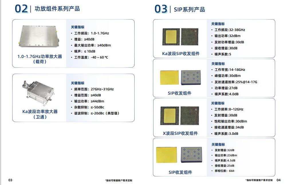
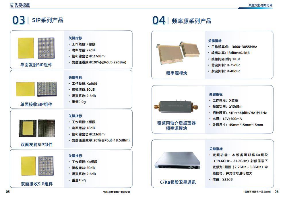
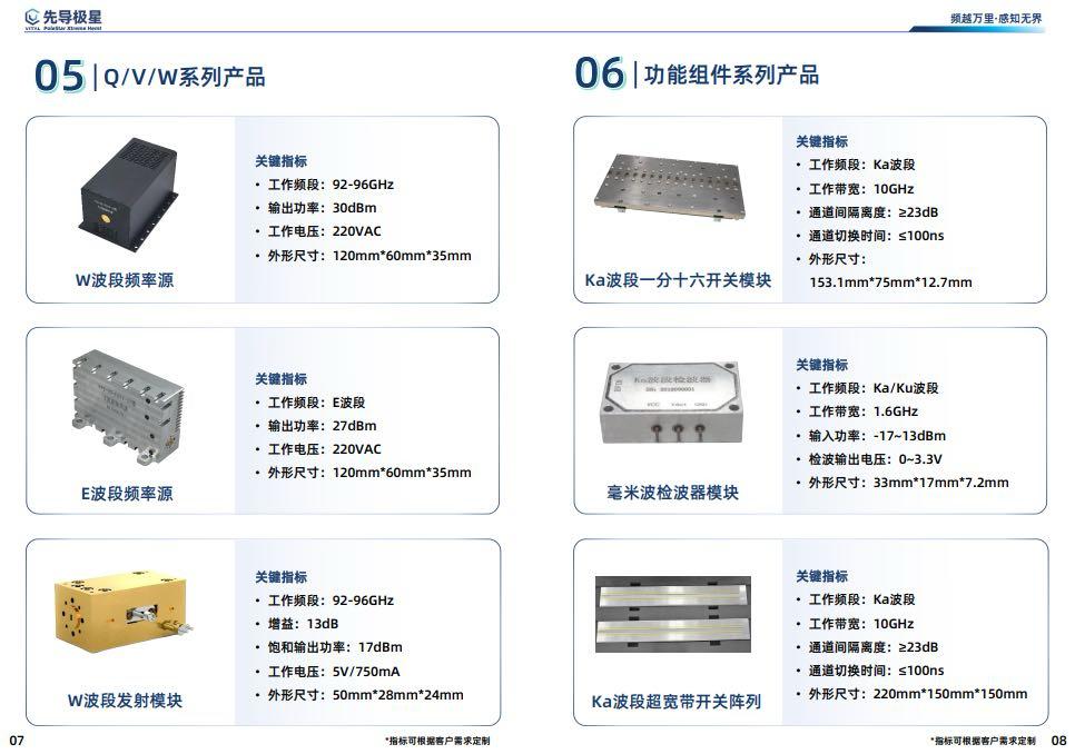
- Anhui Xiandao Jixing X-band GaAs pHEMT drivers and medium-power MMICs cover 8–12 GHz at 20–25 dBm P1dB with a low noise floor and good linearity, suited to a driver-plus-final two-stage cascade. Their key advantage is small temperature drift and good batch consistency, which matters directly for 4T channel amplitude and phase matching.
- GaN HEMT MMICs from Xiamen Lingyang Huaxin and Suzhou Nengxun reach 30–33 dBm (1–2 W) at 30–40% efficiency. But GaN shows pronounced memory effects: across a 300 MHz sweep, gain varies ±1.5 dB with frequency and needs predistortion plus segmented ALC. GaN gate leakage also rises exponentially with temperature, so static current can double when hot and gate current monitoring is mandatory.
- Vanchip X-band small-power MMICs, born from handset PAs, are extremely cost-effective at under 20 CNY per die for 20 dBm P1dB. The trade-offs are higher noise figure (3–4 dB, irrelevant in a transmit chain) and average EVM (irrelevant for FMCW).
Selection experience:
- Do not worship the P1dB number. Look at the gap between Psat and P1dB: under 2 dB means soft compression (GaAs), over 4 dB means hard compression (GaN). Counter-drone radar wants the end of the linear region, so soft-compressing GaAs is the better fit and delivers about 10 dB better IM3.
- Look at S22. Poor output match means antenna or isolator variation directly shifts the PA operating point. Require S22 below -8 dB across the band.
- Look at video bandwidth. The FMCW chirp envelope is a triangle wave, so video bandwidth must exceed 10 MHz or the chirp rising edge is filtered away and the waveform distorts.
- Look at ESD and HBM ratings. Bare MMIC dies often tolerate only 200 V HBM on the gate, so surrounding ESD parts must bring the assembled board to 2 kV. Assembly floors need grounded wrist straps and ionizers running.
Matching topologies. PA input and output matching is not a 50 Ω pass-through; it means pulling the load to the optimum power circle. Three practical options:
- Topology A — L-section lumped matching (below 3 GHz or on-die): series L plus shunt C transforms 50 Ω to Zin = 25 – j15 Ω taken from load-pull data. The drawback is that at 10 GHz the inductor is only 0.8 nH, and parasitics eat it alive.
- Topology B — quarter-wave transformer (microstrip, recommended): a λ/4 line with Z0 = √(50 × Z_opt), where Z_opt is typically 20–30 Ω. On RO4350B, λ/4 at 10 GHz is about 4.6 mm. It is wideband, low loss, and measurable.
- Topology C — multi-section LC plus transmission line (best for wideband): on the input side, DDS output → RC filter (22 Ω + 100 pF, 70 MHz cutoff, suppressing DDS images) → 1:1 balun → λ/4 microstrip (Z0 = 35 Ω) → PA input. On the output side, PA output → λ/4 microstrip (Z0 = 35 Ω) → harmonic trap (L = 1.2 nH, C = 0.8 pF, resonant at 2f0 = 19.4 GHz) → -20 dB directional coupler → isolator → antenna. The trap location matters: it must sit within 1 mm of the PA output, or the 2f0 trace itself becomes a small antenna and radiates harmonics, taking the whole unit’s EMI down with it.
LNAs — the ears of the system
Requirements: NF ≤ 2 dB, gain ≥ 20 dB, OIP3 ≥ +5 dBm to avoid compression from close-in high-power targets, input P1dB ≥ -5 dBm, and S11 < -10 dB.
- CETC Institute 55 CGY-series GaAs pHEMT LNA MMICs: NF 1.2–1.8 dB, gain 22–28 dB, OIP3 +8 to +12 dBm — an industry benchmark. The input stage is the most fragile part, so the bias sequence must be Vg negative first, then Vd, with a soft Vd ramp.
- Anhui Xiandao Jixing X-band LNAs strike a good balance between NF and linearity at 1.5–2.0 dB and OIP3 above +5 dBm, well suited to weak-signal reception in strong-interference environments. Pairing their GaAs PIN limiter ahead of the LNA lets the input survive 100 mW of continuous leakage without desensitizing.
- Maxscend handset-derived LNAs offer 1.8–2.2 dB NF and 18 dB gain under 10 CNY, but their OIP3 is only around 0 dBm, so they compress easily against close-in strong targets in counter-drone use. Use with caution.
- SmarterMicro reconfigurable LNAs support band switching, which suits multi-role export models.
Matching: the LNA input must match Γ_opt, the optimum noise reflection coefficient, not 50 Ω — the most common beginner mistake. Γ_opt usually sits in the capacitive region of the Smith chart. The chain is antenna → shunt ESD diode → series microstrip inductance (about 1.5 nH, roughly 2 mm of line) → LNA input (Zin = 35 – j20 Ω), then LNA output → 100 pF AC coupling → 50 Ω microstrip → image-rejection filter. The deliberate mismatch on the input side trades 0.3–0.5 dB of noise figure for S11 degrading to -7 dB. Noise figure wins over return loss, because NF multiplies directly into the radar equation.
Mixers and I/Q demodulators
Requirements: LO-RF isolation > 40 dB, IIP3 > +10 dBm, conversion loss < 8 dB, amplitude balance ±0.5 dB, and phase balance ±5°.
- CETC Institute 41 and Institute 13 GaAs double-balanced mixers: 7 dBm LO drive, 6–7 dB conversion loss, +15 dBm IIP3.
- Anhui Xiandao Jixing I/Q demodulator MMICs hold good amplitude and phase balance (±0.3 dB, ±3°) across 8–12 GHz, which is the key to 60 dB image rejection. Combined with their wideband vector voltage attenuator for I/Q mismatch calibration, image rejection improves by another 15 dB.
- Analog Devices ADL5380 and ADL5375 remain the benchmark, but domestic pin-compatible replacements are not fully compatible: the ADI Vset pin is voltage-controlled attenuation while most domestic parts are current-controlled, so the bias network must change.
A production-ready I/Q mismatch calibration method: first run a board-level loopback (transmit chirp → coupler → receive) to inject a signal with known amplitude and phase. Then have the FPGA capture the I/Q data and apply a complex rotation, Z_cal = (I + jQ)·(a + jb), solving for a and b that minimize the image. Burn a and b into each board’s SPI flash as a factory calibration, then compensate temperature drift with a three-point (-40/25/70 °C) lookup table. This step must be part of the production process, or 30 of every 100 units will ship with image rejection below 30 dB and come straight back.
PLL, VCO, and OCXO — the local oscillator chain
Requirements: phase noise -95 dBc/Hz at 1 kHz, -105 at 10 kHz, -110 at 100 kHz, and -130 at 1 MHz; spurious below -70 dBc; lock time under 100 μs to support frequency-hopping countermeasures.
- PLL: parts from Zhenxing Technology (a Goertek subsidiary), Chengchang Technology, or Guobo Electronics. When replacing the ADI ADF5610, note that the charge-pump current programming range differs — domestic parts often span 0.5–4 mA against ADI’s 0.3–12 mA — so the loop bandwidth must be recalculated.
- VCO: Anhui Xiandao Jixing X-band VCO and ODC devices reach -110 dBc/Hz at 100 kHz with a pushing figure under 50 MHz/V. Keep the push-push figure below 5 MHz/rad, or PA AM noise couples through the supply into the VCO and creates supply-induced FM that bulges the 10 kHz phase noise.
- OCXO: 100 MHz oven-controlled oscillators from Beijing Dahua, Wuhan Haocheng, or Zhejiang Dongjing reach better than -150 dBc/Hz at 1 kHz with aging below 5e-10 per day. Note that export models may face licensing requirements for high-precision clocks in some countries, so confirm with trade compliance early.
- Jitter cleaner: a TI LMK04828 or a domestic clock chip from NOVOSENSE or 3PEAK to distribute JESD204B SYSREF and device clocks with jitter under 200 fs.
Loop filter design. Choosing the PLL loop bandwidth fc is a trade between phase noise and spurious response. Below 10 kHz, VCO phase noise dominates (good) but reference spurious is not filtered (bad) and lock time grows. Above 100 kHz, reference spurious is clean (good) but PFD and divider noise are amplified (bad). The sweet spot for counter-drone radar is fc = 20–30 kHz with 50–60° phase margin, using a third-order passive RC network plus an op-amp for active filtering. One worked example: R1 = 1.2 kΩ, C1 = 47 nF, R2 = 12 kΩ, C2 = 4.7 nF, C3 = 470 pF, with a low-noise op-amp such as 3PEAK TP226x at 1.1 nV/√Hz. C3 is the secret weapon — it lifts the third-order loop’s phase margin from 35° to 55°, which directly determines lock time and overshoot.
ADC, DAC, and DDS
Requirements: ADC 16-bit, ≥ 65 MSPS, SNR > 75 dB, SFDR > 85 dB; DAC/DDS 14–16 bit, update rate ≥ 1 GSPS, spurious < -80 dBc.
- ADC: 3PEAK TPAD92x series at 16-bit, 65/80/105 MSPS; NOVOSENSE SAR ADCs for monitoring; CETC Institute 24 high-speed ADCs, with 16-bit 65 MSPS in volume production. When replacing the AD9265, note that the digital output is 1.8 V LVDS, not 3.3 V CMOS, so the FPGA bank voltage must change.
- DAC/DDS: Zhenxing Technology and Guobo Electronics DDS parts. A DDS IP core inside a Puzhoutongchuang FPGA can also generate chirps, but its phase noise and spurious performance trail dedicated DDS parts, so it suits only coarse sweeping in a jamming module. A drop-in domestic replacement for the ADI AD9164 does not exist yet, so if the customer accepts a non-fully-domestic BOM, keep that one part and localize the rest.
- JESD204B: domestic FPGAs from Puzhoutongchuang (Logos), Anlogic (Phoenix), and Fudan Microelectronics (JFM) support JESD204B Subclass 1 with 6.25 Gbps PHY rates. The alignment of SYSREF is the number one production trap: when 5 of 100 boards fail link establishment, 90% of the time the SYSREF skew exceeds 500 ps. Fix it with a global clock tree, ±50 mil length matching, and software-based SYSREF capture calibration on the FPGA side.
FPGA — choosing the brain
Requirements: transmit and receive timing control (32 channels × 100 μs chirp, jitter < 10 ns), DDC (16 channels × 65 MSPS), FFT (1024–4096 points), CFAR (cell-averaging or ordered-statistic), MHT track association, JESD204B, DDR3/4 buffering, and gigabit Ethernet point-cloud output.
- Puzhoutongchuang Logos-2 (PG2L100H and PG2L160H): roughly 100K–160K LUTs and 400–600 DSP blocks, with JESD204B, DDR3 controllers, and 6.25 G SerDes. The value leader at 300–600 CNY per part, well suited to channel processing plus interfaces.
- Anlogic Phoenix (PH1A/B): 50K–200K LUTs with rich DSP resources and a mature TangDynasty toolchain. The limitation is a 5 G SerDes ceiling, so JESD204B can only run Subclass 0, which is unfriendly to multi-ADC synchronization.
- Fudan Microelectronics JFM series (space grade): mandatory for satellite-borne or space-based counter-drone work, with radiation tolerance and a -55 to +125 °C range, but at ten times the price of commercial parts and a six-month lead time.
- Guowei Electronics SoC FPGAs with ARM hard cores suit integrated radar-plus-AI-classification units.
A rough sizing formula: DSP48 demand is about 8 DSP blocks per channel (two complex multiplies in the DDC, four real multiplies in the FFT, two comparisons in CFAR), so 16 channels need about 128, and with 50% margin you want at least 200. BRAM demand is 16 channels × 4096 points × 16 bit × 2 for I/Q, about 2 Mbit, doubling to at least 4 Mbit with margin. LUT demand for state machines, interfaces, and control is about 60K. The conclusion: pick a part with at least 100K LUTs, 400 DSP blocks, and 4 Mbit BRAM — PG2L100H sits right on the line and PG2L160H is comfortable.
Counter-drone-specific logic design points: use double buffering with preload for chirp timing so the next chirp’s parameters are already in SRAM while the current one runs, holding jitter under 5 ns. Build the DDC as three stages — complex mixing, CIC decimation by 16 (65 to 4 MSPS), then FIR shaping (4 to 2 MSPS) — followed by a 1024-point FFT. Use cell-averaging CFAR with leading and trailing guards, 32 reference cells and 4 guard cells, a false-alarm probability of 1e-6, and a threshold factor near 12.5. For MHT, use multi-hypothesis tracking with probabilistic data association, 8–16 hypotheses, tracks surviving five frames and deleted after three, associating zero-velocity targets in range-azimuth-elevation without relying on Doppler. Store calibration data in QSPI NOR flash (GigaDevice GD25 or Winbond W25 equivalents) so it loads within 200 ms of power-up.
Passives — small parts, big traps
- RF bypass capacitors: Fenghua Advanced 0402 100 nF NP0/C0G with self-resonance above 3 GHz and ESR below 0.1 Ω. Never use X7R for RF bypass: its capacitance drifts -30% under bias, so 100 nF becomes 70 nF at 10 V and the resonance moves.
- Bulk supply capacitors: Aishi or Jianghai polymer aluminum electrolytics at 100 μF/10 V with ESR below 30 mΩ and ripple current above 1 A.
- DC blocking: C0G 0402 from 100 pF to 1 nF at LNA and PA inputs and outputs.
- Tuning capacitors: Skyworks or Maxscend GaAs varicaps, or Xiandao Jixing varactor diodes, at 0.5–5 pF with Q above 200 at 10 GHz.
- RF chokes: Sunlord 0402 6.8 nH wire-wound inductors with Q above 30 at 2 GHz, self-resonance above 8 GHz, and DC resistance below 0.3 Ω. Never use multilayer inductors as RF chokes — their self-resonance is only about 3 GHz, so they behave as capacitors at 10 GHz.
- Power chokes: Microgate molded inductors at 10 μH/2 A with DCR below 50 mΩ.
- RF attenuators and terminations: Yageo or Fenghua 0402 thin-film resistors with TCR below 50 ppm for PA gate dividers and ADC front-end attenuation.
- Current sensing: a TI INA226 or NOVOSENSE NSD731x with a 0.1 Ω sense resistor at 0.1% accuracy.
- Ferrite beads: Sunlord or Microgate 0603 beads at 600 Ω at 100 MHz and still above 200 Ω at 1 GHz. Placing one in series with the LNA Vd supply alongside a 10 μF capacitor suppresses DC-DC switching noise by another 20 dB.
- RF connectors: SMP/SMPM board-to-board connectors from CETC Institute 40 or HuaDa, rated to 40 GHz with insertion loss below 0.3 dB. Avoid SMA for board-to-board use — too bulky and it fails after repeated mating.
- Antennas: array antennas laminated from four layers of Rogers RO4350B with RO4450F prepreg, εr = 3.66, 0.508 mm thick. Patch spacing is λ/2 = 15 mm, an 8-element array is 120 mm long and a 4-element row is 60 mm wide, which fits inside an 840 × 680 × 320 mm enclosure.
- Absorber: ECCOSORB-type foam from Dalian Yibang or Langpuda on the cavity walls to suppress cavity resonances, since at 10 GHz a λ/2 cavity mode is about 15 mm and a small cavity is effectively a filter.
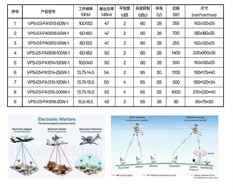
Frequency-Agile Wideband PAs
“Frequency-agile wideband” is the high-value corner of counter-drone jamming and satellite or data-link RF. It does not mean simply tunable frequency; it means wide instantaneous bandwidth plus a hopping center frequency, both at once. Counter-drone jamming needs wide coverage; satellite and data links need hopping for interference avoidance and low probability of intercept.
Three amplifier classes compared:
- Class A (linear): 360° conduction angle, 10–20% efficiency, best linearity (IM3 < -40 dBc). Suited to deception jamming and data links where the modulation waveform must be preserved, and to counter-drone radar transmit chains.
- Class AB (compromise): 180–360° conduction angle, 30–50% efficiency, moderate linearity (IM3 -25 to -30 dBc). Suited to narrowband barrage jamming.
- Class C and E (switching): 60–80% efficiency but severe nonlinearity. Only usable for continuous-wave barrage and RF heating, never for any modulated signal.
Three make-or-break wideband PA specs:
- Gain flatness: ±1 dB across 300 MHz is passing, ±0.5 dB is excellent. Degradation comes from input and output match failing at band edges, which rolls off S21. Fix it with multi-section λ/4 transformers and lossy matching.
- Output power (P1dB and Psat): 20 dBm (100 mW) to 33 dBm (2 W). GaAs pHEMT reaches P1dB around Ids = 0.7·Idss and GaN around Vgs = Vth + 2 V. During bring-up, hand-tune Vgs to find the bias point with maximum P1dB, then freeze it as a resistor divider value.
- Efficiency (PAE and drain efficiency): counter-drone radar transmits continuously, so efficiency determines thermal design. PAE = (Pout – Pin)/Pdc. Three ways to raise it: dynamic bias (drop Vd at low power), Doherty architecture (about +10% backoff efficiency), and envelope tracking. Doherty is buildable at X-band but needs a peak PA, a carrier PA, a 90° hybrid, and impedance transformation, doubling layout area — not recommended for cost-sensitive export models, but usable in high-end space applications.
Two hidden traps in frequency-hopping amplifiers. First, transient shock during frequency switching: if the PLL hops within 100 μs but the PA gate bias responds slowly (RC time constant above 10 μs), the start of the chirp shows a gain notch and the waveform distorts. Set the gate RC time constant to 2–5 μs (R = 10 kΩ, C = 220 pF) and silence the first 2 μs of each chirp in the FPGA. Second, harmonics wander with frequency: 2f0 moves between 18.8 and 19.4 GHz, and a fixed LC trap only suppresses the center. Use distributed harmonic suppression instead — place a 0.5 pF shunt capacitor every λ/4 at 2f0 (about 2.3 mm) along the PA output microstrip to form a harmonic-shorting transmission line that absorbs 2f0 energy along its whole length.
Moving from 10 Units to 1,000
Three mass-production killers
- Device batch drift. The same LNA model can differ by 0.5 dB in NF and 2 dB in gain between wafers. Sample S-parameters and NF on every incoming batch, build a batch-to-parameter database, and load FPGA calibration tables by batch.
- PCB dielectric drift. RO4350B is specified at εr = 3.66 but measures 3.55–3.75. Require a TDR report from the board house per batch and leave adjustable pads (0 Ω positions plus 1 pF positions) in the matching network so the BOM can change when deviation is large.
- Assembly consistency. SMP connector locking torque, thermal grease thickness, and shield-can grounding finger pressure all shift RF performance. Fix them all with fixtures, torque screwdrivers, and application templates, and quantify them in the work instruction.
RF-specific incoming quality control
- MMICs (PA, LNA, mixer): 100% S-parameter test with an automated VNA under 10 s per part, screening out S21 deviations beyond ±2 dB; sample P1dB, NF, and OIP3 at five per batch.
- VCO and OCXO: 100% phase-noise test under 20 s per part, screening out anything above -100 dBc/Hz at 10 kHz.
- Capacitors and inductors: sample self-resonance, Q, and tolerance with an LCR bridge and impedance analyzer.
- PCB: 100% impedance coupon test by TDR, 50 Ω ±10% and 100 Ω ±10%.
- Mechanical parts: 100% inspection of cavity dimensions, shield-can grounding finger pressure, and heat-sink flatness below 0.05 mm.
Calibration and test fixtures
- Board-level calibration jig: pogo pins plus locating pins in a single press, automatically measuring amplitude, phase, and bias across 12 channels, then writing the calibration table to QSPI flash in under three minutes per board.
- Chamber testing: a microwave anechoic chamber (absorber with reflection below -40 dB at 10 GHz) plus a target simulator and turntable, measuring the three-dimensional range-azimuth-elevation curve in under 15 minutes per unit.
- Automation software: Python plus LabVIEW plus VISA driving signal sources, spectrum analyzers, power meters, VNAs, oscilloscopes, and thermal chambers to produce a test report, calibration data, and pass/fail verdict in one run, tied into MES.
Debugging batch-level deviations
A fault tree for the most common symptoms:
- Whole batch loses 3 dB of P1dB: check the PA gate divider resistors (a batch error drifting Vg by 0.1 V costs 3 dB) and switch to 0.1% thin film; check Vd ripple (DC-DC inductor saturation at 200 mV ripple compresses gain) and switch to molded inductors; check heat sinking (thin thermal grease raises junction temperature 20 °C and costs 2 dB) and add application templates plus weight checks.
- Whole batch gains 1 dB of NF: check LNA Vg drift; check ESD damage (assembly floor humidity below 30% punches through LNA gates for 2 dB) and enforce EPA zones, ionizers, and wrist straps; check image-filter insertion loss (BAW batch variation from 2 to 4 dB) and switch to SAW or LTCC, or raise LNA gain from 20 to 22 dB.
- Whole batch shows a 5 dB phase-noise bulge at 10 kHz: check the VCO supply (DC-DC harmonics at 1.5 MHz coupling in) and add a bead plus 10 μH choke; check PA AM noise coupling through a shared supply and split the rails with a ground wall; check the reference clock (OCXO aging adding 3 dB) and test phase noise 100% on incoming inspection.
- Whole batch image rejection below 30 dB: check I/Q demodulator amplitude and phase balance batch drift and run digital calibration in the factory; check LO distribution length differences and match the four LO lines within ±2 mm.
- 5% JESD204B link failures: check SYSREF skew and use a global clock tree with ±50 mil matching plus FPGA-side calibration; check SerDes via count (more than two vias creates an impedance discontinuity) and revise the layout.
Ten cost-reduction levers
Export models compete on BOM, so cut cost without cutting specs:
- Replace GaN with GaAs in the PA — 100 mW is enough for counter-drone radar transmit, and GaN’s 2 W is waste. Saves about 80 CNY per die.
- Replace ADI LNAs with domestic parts from CETC Institute 55 or Xiandao Jixing instead of the ADL5523. Saves about 60 CNY each across 8 channels, or 480 CNY.
- Replace the AD9265 ADC with 3PEAK, NOVOSENSE, or CETC Institute 24 parts. Saves about 40 CNY each across 16 channels, or 640 CNY.
- Replace the Xilinx Zynq-7020 with a Puzhoutongchuang Logos-2 PG2L100H. Saves about 300 CNY.
- Replace imported OCXOs with Beijing Dahua or Wuhan Haocheng parts. Saves about 200 CNY.
- Replace TE or Rosenberger connectors with CETC Institute 40 SMP/SMPM parts. Saves about 50 CNY per set.
- Replace Coilcraft or Murata inductors with Sunlord or Microgate parts. Saves about 0.5 CNY each across 200 parts, or 100 CNY.
- Replace TDK or Samsung capacitors with Fenghua Advanced parts. Saves about 0.02 CNY each across 1,000 parts, or 20 CNY.
- Use RO4350B only on the RF layer and FR4 elsewhere in a hybrid stackup. Saves about 300 CNY.
- Switch from CNC aluminum to die-cast aluminum above 500 units. Saves about 200 CNY per enclosure.
The total is roughly 2,500 CNY per unit, or 2.5 million CNY across 1,000 units. That is the value an RF chief engineer delivers.
Domestic sourcing list
For a directly usable BOM localization report: PA MMICs from Anhui Xiandao Jixing (X-band GaAs pHEMT) and CETC Institute 55/13 (CGY series); LNA MMICs from CETC Institute 55 and Xiandao Jixing; vector voltage attenuators, limiters, and switches from Xiandao Jixing and CETC Institute 13/55; mixers and I/Q parts from CETC Institute 41/13 and Xiandao Jixing; VCO and OCXO from Xiandao Jixing, Beijing Dahua, Wuhan Haocheng, and Zhejiang Dongjing; PLL and clock parts from Zhenxing Technology, Chengchang Technology, Guobo Electronics, NOVOSENSE, and 3PEAK; ADC, DAC, and DDS from 3PEAK, NOVOSENSE, CETC Institute 24, Zhenxing Technology, and Guobo Electronics; FPGAs from Puzhoutongchuang Logos-2, Anlogic Phoenix, and Fudan Microelectronics JFM for space; capacitors from Fenghua Advanced, Aishi, and Jianghai; inductors and ferrite beads from Sunlord and Microgate; connectors from CETC Institute 40 and HuaDa; PCBs from Shennan Circuits, WUS, Kinwong, and Shengyi Technology; thermal and sealing materials from Zhonglan Chenguang and Huitian New Materials; absorber from Dalian Yibang and Langpuda; and test instruments from Ceyear (CETC Institute 41), RIGOL, SIGLENT, and UNI-T. Device-count localization exceeds 95% and value localization exceeds 85%, with the FPGA and high-end ADC the last two gaps being closed by Puzhoutongchuang and CETC Institute 24.
Traceability: the last mile of production
When export models ship, customers ask less about specifications and more about consistency, reproducibility, and whether a problem can be traced back to a wafer. Four things are mandatory on the line. Every board carries an identity: a 32-byte unique ID burned into QSPI flash from wafer lot, die position, production date, and serial number, with test data stored server-side and readable by the customer via QR code. Every curve is archived: P1dB, NF, phase noise, S-parameters, and channel consistency, about 12 plots per unit, roughly 5 MB compressed, so a machine’s whole life is on record. Calibration tables are versioned: FPGA I/Q calibration, PA temperature compensation tables, and LNA gain corrections all carry a version number and applicable batch, and changing batch requires a version bump — never quietly edit the numbers. Failure analysis closes the loop: every returned unit gets X-ray, decapsulation, layer removal, and SEM within 72 hours, with root causes classified as design, device, process, incoming material, or operation, and reviewed monthly.
Three problems that only appear in production
- “A machine that passes in summer loses 2 dB in winter.” At +70 °C, P1dB drops 2–3 dB and customers in Dubai or Saudi Arabia complain. The GaAs pHEMT P1dB temperature coefficient is only about -0.02 dB/°C; the real culprit is the matching capacitor’s temperature coefficient — X7R is ±15% — so capacitance falls 15% when hot, resonance shifts 7%, return loss goes from -15 to -8 dB, and P1dB drops 2 dB. Fix it by switching all matching capacitors to C0G/NP0 (±30 ppm), using thin-film 0.1% 50 ppm resistors for the PA gate divider, and adding a temperature-compensation table measured at -40/25/70 °C with 1.5 dB of digital predistortion compensation in the FPGA.
- “Three boards in the same batch bulge at 10 kHz.” Three of 100 units show 5 dB higher phase noise at 10 kHz and lose 5 dB of hovering-target SNR. The cause is the VCO tuning line running parallel to the PA VDD switching node for 3 cm, coupling into the tuning diode and creating supply-induced FM. Fix it by routing the VCO tuning line as coplanar waveguide with ground walls, crossing all digital and power traces perpendicularly, adding a 10 μH choke plus a 600 Ω at 100 MHz bead plus 100 nF C0G on the VCO supply, and adding a 10 kHz phase-noise item to incoming inspection at 100% coverage.
- “JESD204B fails to link 5% of the time, intermittently.” At -40 °C the failure rate rises to 20%. The cause is a 200 mil SYSREF length difference; at low temperature the FPGA capture window shrinks and the sample point lands on the eye edge. Fix it with a global SYSREF clock tree, ±50 mil matching, and software calibration that runs an eye scan to find the optimum sample point and stores it in flash.
Export compliance checklist
Compliance is a matter of survival for counter-drone exports, and the technical lead has to gate it at the proposal stage. Verify the target country’s spectrum rules for ISM and license-exempt bands and power limits (FCC Part 15 and Part 90 in the US, RED in the EU, TDRA in the UAE, CST in Saudi Arabia). Treat jamming functions as regulated — active suppression and deception require a radio operating license in most countries, and spoofing civilian GPS is prohibited — so build jamming modules as optional, removable, default-off at 0 dBm, unlockable only with authorization, and logged for audit. Check encryption and export controls, since high-precision OCXOs, radiation-tolerant FPGAs, and high-power GaN devices may fall under dual-use lists. Meet EMC and EMI requirements such as CE and FCC Part 15B with 6 dB of margin below radiated limits, and cover environmental and safety rules including IP rating, salt spray, RoHS, and REACH. Documentation must include an English BOM, an English test report, an English calibration certificate, and a CE declaration of conformity.
Advanced Topics: Satellite, Data Link, and Wideband PAs
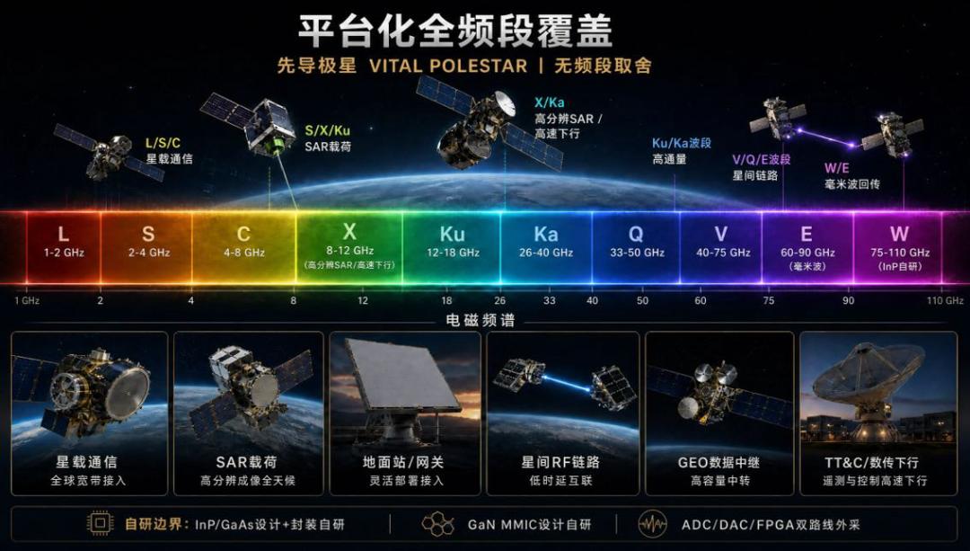
Counter-drone jamming, counter-drone radar, satellite payloads, data links, and frequency-agile wideband amplifiers all rest on the same RF and microwave physics; only the weighting of the specifications changes.
Satellite-borne payloads
- Radiation tolerance: total ionizing dose above 100 krad(Si) and single-event latch-up immunity above 75 MeV·cm²/mg. Choose JFM FPGAs from Fudan Microelectronics, radiation-hardened MMICs from CETC Institute 55, and space-grade VCOs and PAs from Xiandao Jixing.
- Temperature: -55 to +125 °C, which rules out COTS parts entirely — capacitor ESR, inductor self-resonance, and crystal aging all shift.
- Power: solar-array powered, so PAE carries the highest weight. PAs must use Doherty plus envelope tracking to lift efficiency from 15% to 35%.
- Reliability: single-event upsets require triple modular redundancy and readback correction in the FPGA configuration.
- Thermal: a vacuum has no convective cooling, so heat must radiate along a die-to-copper-carrier-to-heat-pipe-to-radiator path with junction-to-case thermal resistance below 5 °C/W.
Data links
- Linearity first: EVM better than -30 dB for 64-QAM OFDM and IM3 below -40 dBc, so the PA must run 6–10 dB backed off from P1dB, trading efficiency for linearity.
- Wideband: 500 MHz to 1 GHz instantaneous bandwidth requires distributed, multi-section λ/4 matching with ±1 dB gain flatness.
- Frequency hopping: 1,000 hops per second demands PLL lock time under 10 μs, achieved with fractional-N synthesis, a wideband VCO, and fast calibration.
- MIMO: 2×2 or 4×4 with channel consistency of ±0.5 dB and ±5°, tighter than counter-drone radar.
Frequency-agile wideband PAs
The core tension is bandwidth versus efficiency versus linearity. Distributed, traveling-wave topologies cover 8–18 GHz with 10 dB gain and ±1.5 dB flatness but only 5–8% efficiency. Switching classes such as Class E and F reach high efficiency, but their resonant networks limit instantaneous bandwidth to about 10%. The compromise now favored in both academia and industry is continuous Class F with harmonic-tuning bandwidth extension, which achieves 40% PAE and -35 dBc IM3 within a 20% relative bandwidth.
Debugging notes: run load-pull with a Focus MPT system or a domestic CETC Institute 41 load-pull setup, tuning fundamental, second harmonic, and third harmonic simultaneously to find the intersection of the power, efficiency, and linearity circles. Then run source-pull to find Γ_opt for linearity rather than for power. Memory effects matter too — baseband IMD degrades IM3 by 10 dB when two tones are spaced under 1 MHz, and that is the superposition of thermal and electrical memory. Counter it with wideband decoupling on the gate bias (0.1 μF polymer in parallel with 100 pF C0G) and active bias on the drain (op-amp plus Darlington).
Closing Thoughts from a Chief Engineer
RF is physics, not software. Changing a 0.5 pF capacitor can move P1dB by 3 dB; drawing one 2 mm trace wrong can bulge phase noise by 5 dB. Keep a healthy respect for Ohm’s law and Maxwell’s equations — that core has not changed in 50 years.
Localization is a necessity, not a slogan. Five years ago a 1 dB noise-figure gap on a domestic LNA was a real concern; today X-band MMICs from CETC Institute 55 and Anhui Xiandao Jixing hold their own against ADI. Knowing how to use domestic parts, being willing to use them, and using them well is the core competence of this generation of RF engineers.
Mass production is about detail, not scale. For 1,000 units, 99% of specification consistency comes from five words: fixtures, work instructions, incoming inspection, calibration, and data traceability. The day you turn debugging experience into production rules is the day you move from engineer to chief engineer.
Have questions about this article? Feel free to contact us at [email protected] — we’re happy to help!
Frequently Asked Questions
What is a counter-drone radar?
A counter-drone radar detects and tracks small unmanned aircraft, typically using X-band FMCW waveforms with a wide field of view. Because small quadcopters have an RCS near 0.01 m², the design emphasizes low receiver noise figure, high channel consistency, and low phase noise rather than raw transmit power.
Why does counter-drone radar need such low phase noise?
Hovering drones have near-zero Doppler, so detection relies on long chirp accumulation. Phase noise becomes a raised noise floor as accumulation grows, directly eating the target. That is why the design targets -95 dBc/Hz at 1 kHz and -110 dBc/Hz at 100 kHz.
How many RF channels does a 4T8R counter-drone radar need?
Four transmit and eight receive antennas create 32 virtual channels through MIMO, but only 12 physical RF channels. Amplitude and phase consistency across all 32 virtual channels must stay within ±1 dB and ±10°, or angle accuracy degrades from about 1° to 5°.
Can counter-drone radar use domestic Chinese components?
Yes, for the great majority of the BOM. Device-count localization exceeds 95% and value localization exceeds 85% using parts from CETC institutes, Puzhoutongchuang FPGAs, 3PEAK and NOVOSENSE converters, and Sunlord or Fenghua passives. High-end ADC and DDS remain the last gaps.
What causes most counter-drone radar production failures?
Batch-level deviation dominates. Device batch drift shifts LNA noise figure by 0.5 dB, PCB dielectric variation from 3.55 to 3.75 breaks matching, and SYSREF skew above 500 ps causes JESD204B link failures. Incoming inspection and factory calibration are the main countermeasures.
About Aomway
Aomway is a technology company specializing in drone and FPV equipment, publishing in-depth analyses of motor control, embedded hardware, and open-source robotics projects. With over 15 years of industry experience, Aomway covers the full spectrum from flight controllers and FPV goggles to thermal imaging cameras and long-range datalinks for the global drone community.